Skip to content
  • FAQ
  • News
  • Contact Us
Logo
 
  • ABOUT THE ARCHIVES
  • ABOUT HEWLETT-PACKARD CO. HISTORY
    • HEWLETT-PACKARD COMPANY HIGHLIGHTS
    • EXECUTIVE LEADERSHIP
    • MERGERS, ACQUISITIONS & SALES
  • LOOK INSIDE THE VAULT
  • EXPLORE THE VAULT
  • FAQ
  • News
  • Contact Us
  • Home •
  • Progress Made in HP Production •
  • Video: Clean Rooms for Semiconductors

Video: Clean Rooms for Semiconductors

Date: ca. 2014
Share this piece of history
Share on Facebook
Facebook
Tweet about this on Twitter
Twitter

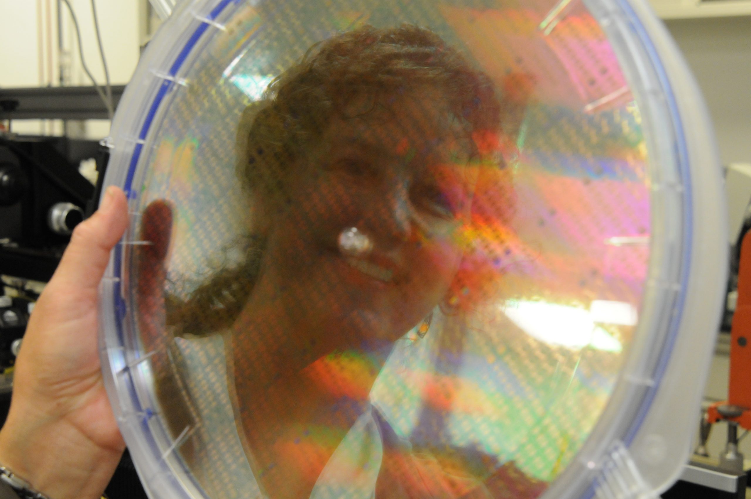
HP Labs built its own clean room in Palo Alto for semiconductor research. The facility was outfitted with a combination of industry standard and in-house technologies that allowed developers to experiment with new materials and designs without requiring the much larger spaces or equipment that many semiconductor companies used.

Tags: 2010s • 2014 • HP Labs • Semiconductor • video

( C ) HPCA

 
Mary Henry Mosaic Mural at HP
 
 
Going for a Dip: Dip-Soldering Circuit Boards
 
Related
Barney Oliver: The Boss of HP Labs
Forty Years of Innovation at HP Labs
Memristors: From Theory to Reality
POWERED BY
Heritage Werks
© 2023 Hewlett-Packard Company Archives. All rights reserved.
HP, Inc. Terms of Use and HPE Terms of Use

  • About the Archives
  • ABOUT HEWLETT-PACKARD HISTORY
    • HEWLETT-PACKARD COMPANY HIGHLIGHTS
    • EXECUTIVE LEADERSHIP
    • MERGERS, ACQUISITIONS & SALES
  • Explore The Vault
Tell Us What You Think Icon
Tell Us What You'd Like To See?
Tell Us What You Think Icon
Tell Us What You'd Like To See?
  • About the Archives
  • ABOUT HEWLETT-PACKARD HISTORY
    • HEWLETT-PACKARD COMPANY HIGHLIGHTS
    • EXECUTIVE LEADERSHIP
    • MERGERS, ACQUISITIONS & SALES
  • Explore The Vault
POWERED BY
Heritage Werks
© 2022 Hewlett-Packard Company Archives. All rights reserved.
HP, Inc. Terms of Use and HPE Terms of Use